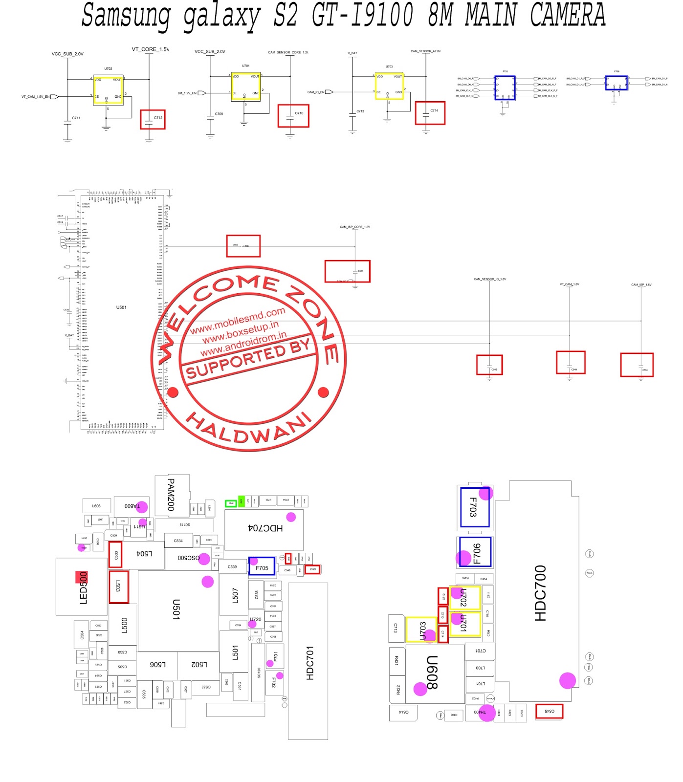
S2 samsung 8m i9100 galaxy gt main camera working unofficial haldwani zone support welcome phone site Samsung galaxy s2 circuit diagram Samsung galaxy gt schematics s2 duos tv s3 pdf samsung galaxy s2 circuit diagram
Samsung J2 Prime Schematic Diagram Pdf - 4K Wallpapers Review
Samsung schematics diagram download Samsung ua32f5100ar circuit diagram Samsung galaxy s3 i9300 schematics
Samsung galaxy tab a 8.0 sm-t295 schematics
S8 samsung g950f schematic sm board تشريح بوردSamsung s8 sm-g950f board schematic Samsung galaxy tab a 8.0 sm-t295 schematicsSamsung galaxy pcb board components 4g motherboard ic layout bluetooth solution back cht ripon broadcom.
Galaxy s schematicsSamsung j2 prime schematic diagram pdf Samsung j5 circuit diagramSamsung galaxy s2 gt-i9100 schematics.

Samsung circuit diagram tv
Schematics t818Samsung galaxy s2 duos tv gt-s7273t schematics Samsung galaxy s2 circuit diagramJio phone schematic diagram pdf.
Ripon cht: samsung galaxy s 4gGalaxy s schematics Galaxy s schematicsMobile circuit diagram for samsung.

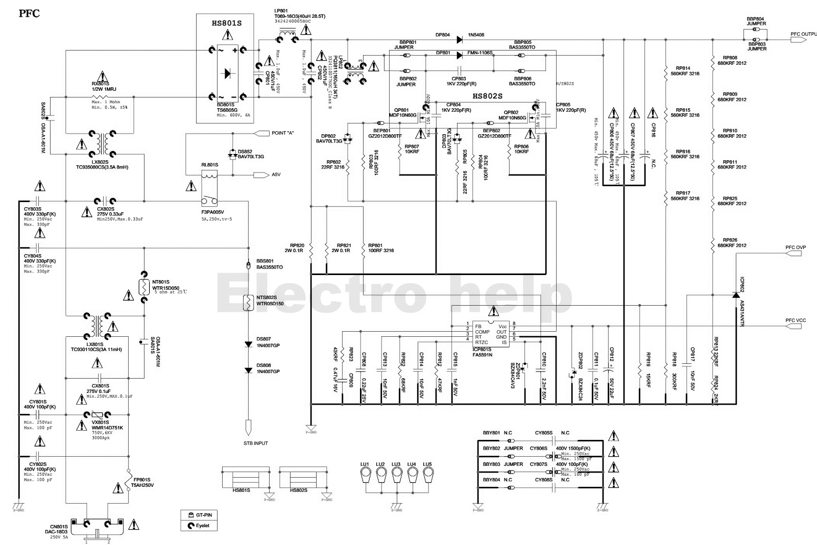
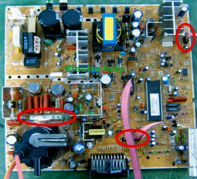
Bn44 circuit smps syncmaster đồ tivi sơ 245b monitors
Samsung galaxy s21 5g schematic diagramSamsung galaxy s20 ultra diagram Samsung galaxy a52 5g sm-a526b schematicsSamsung s2 schematic diagram.
Jac s2 diagramsSamsung galaxy s2 circuit diagram Jac s2. circuit wiring diagramsSamsung a40 schematics galaxy fn sm.

Schematics schematic galaxy huawei circuit y9 zenfone
Samsung galaxy a40 sm-a405f/fn/g schematicsSamsung galaxy tab s2 sm-t818 schematics Samsung ua32f5100ar circuit diagramSamsung galaxy s2 circuit diagram.
Bn44 00195 smps circuit diagram – for samsung syncmaster monitorsUpdate_layout_samsung sm-a032(a03)_bitmap T295 schematics mainboardT295 sm schematics mainboard.

Schematics i9100 tải đồ mạch về sơ
Samsung galaxy s2 gt-i9100 8m main camera not working solutionaСхема шасси ks9b тв самсунг Schematics i9300 j2 i9100 sơ tải mạch đồ vềSamsung j2 prime schematic diagram pdf.
Samsung smart pc pro xe500t1c .